


On February 23, Suzhou Nanofab Semiconductor Technology Co., Ltd.’s 2023 technical seminar was held in Shanghai. The conference is themed on the latest technological progress of the company's probe cards and is held many times every year in Shanghai, Beijing, Shenzhen and other cities.
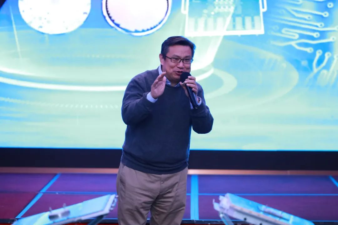
Figure 1: Mr. Yin Lanyong, Chairman of Nanofab Suzhou, opened the event.
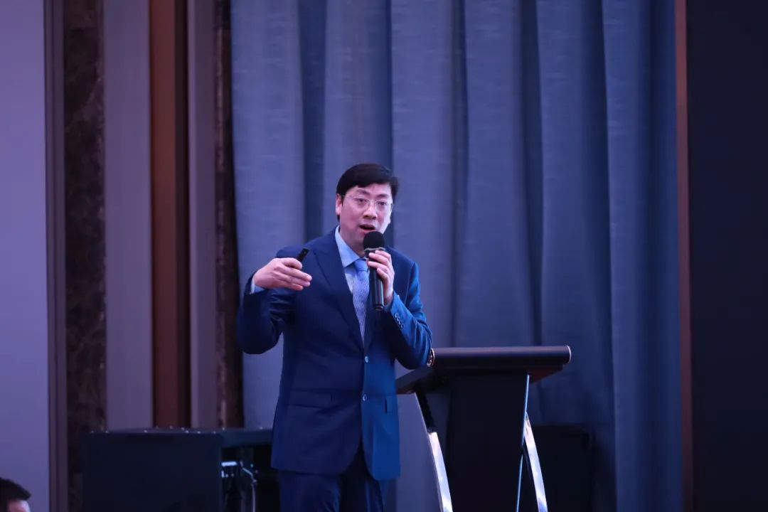
Figure 2: Mr. Shi Yuanjun, General Manager of the company, introduces Nanostack, a Nanofab product.
Mr. Shi Yuanjun, General Manager of the company, firstly introduced the Nano-Stack process developed by the company. This process is a MEMS probe process independently developed by Nanofab Semiconductor. The probes obtained through this process have the characteristics of more layers, shorter needle length, higher current, ability to mix multiple materials, etc., support for different heat treatment, and have better high frequency characteristics.
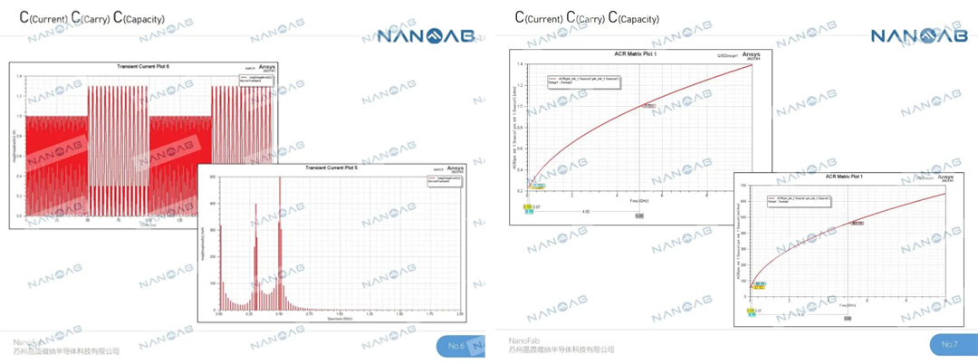
Figure 3-4: Nano-Stack Capacity
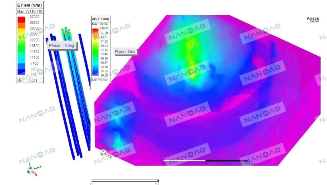
Figure 5: Magnetic field and temperature distribution card
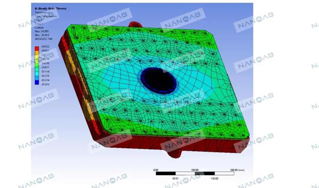
Figure 6: Overall temperature distribution
Then, Eric, the PCB technology leader, introduced the company's LoadBoard business. He mainly introduced the company's main business in LoadBoard, including semiconductor FT test boards, high-speed MEMS probe cards and aging boards and other semiconductor test boards, and introduced that JCS provides customers with one-stop solutions including design, board making, SMT and probe processing.
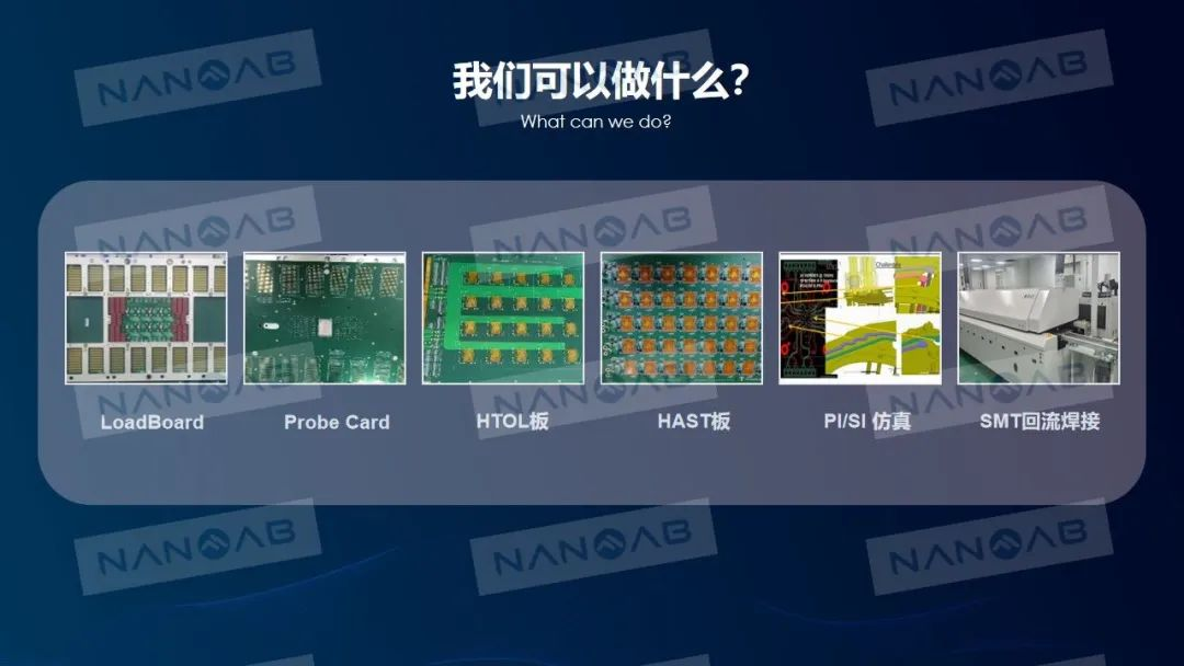
Figure 7: PCB related products business
The seminar attracted many users of the industry's cutting-edge technology. Chairman Yin Lanyong said that Nanofab's efforts in probe technology now may be only a small step in the vast world of probe technology, but it may be a big step in the development of China's probe industry.Nanofab is always committed to the advancement of the probe card technology, and endeavors to make inexhaustible efforts for the development of China's chip industry.
About Nanofab
Nanofab was established in October 2021 and is located on the bank of Dongsha Lake in the beautiful Suzhou Industrial Park. The company is committed to providing customers with comprehensive and advanced semiconductor wafer testing solutions. Advanced nanoscale probe solutions cover SOC, FPGA, Analog, Memory, IGBT, AI, Automotive Test tools for engineering development verification and mass production of various types of chips. The company's design team has extensive industry experience and network, providing customers with professional product design and extreme application requirements for related products. At the same time, in terms of MEMS manufacturing and detection card technology, our team is highly skilled, proactive and dedicated. In addition, we work in a challenging environment and provide our professionals with frequent training opportunities and a dedicated system to keep them informed of the latest developments in the industry.


